
HDI from 1+N+1 to any-layer, built on up to six lamination cycles
0.075 mm laser vias, 3/3 mil lines and stacked or staggered microvias. The build-up is modelled before release, so the impedance holds on the first article.
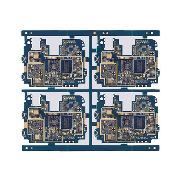
At a glance
- Zoran builds HDI from 1+N+1 up to any-layer, with up to six sequential lamination cycles.
- Minimum laser via is 0.075 mm (0.05 mm best-in-class) and minimum line/space is 3/3 mil (2/2 mil on review).
- Both stacked and staggered microvia stack-ups are supported, including via-in-pad with filled and capped vias.
- An 8-layer any-layer board (1+6+1) with 0.1 mm microvias and 3/3 mil routing is in stable volume production for communication equipment.
- HDI is produced at the Zhongshan plant alongside rigid multilayer, under the same IATF 16949 and ISO 13485 systems.
HDI parameters
Microvia stack-ups: staggered, stacked, and any-layer. Via-in-pad is filled with conductive or non-conductive paste and capped, then planarised before the next lamination.
What decides whether HDI yields
Laser drilling, not mechanical cheating
UV laser drilling to 0.075 mm with energy profiled per dielectric thickness. Mechanical drilling a 0.1 mm hole through FR-4 produces a via wall that fails thermal cycling — it looks right and fails later.
Via fill and planarisation
Via-in-pad is filled, cured and planarised to a flatness that allows 0.35 mm pitch BGA placement. Uneven fill is the most common cause of solder voids on HDI assemblies, and it is a process step, not a design fix.
Any-layer build-up control
Each lamination is registered to target and scaled independently. On six-cycle builds the cumulative registration error, not the single-layer accuracy, determines whether the board passes AVI.
Impedance on 3/3 mil traces
At 0.075 mm line width the impedance is far more sensitive to etch variation, so we control etch compensation per panel and verify on coupon. ±10% standard, ±5% on review.
Sequential lamination without delamination
Brown oxide, press profile and material match are set per stack-up. Mixing FR-4 with low-Dk material on an HDI build is where delamination appears, and where most suppliers quietly decline the order.
Test access on dense designs
Flying probe with fine-pitch fixtures, plus AVI for surface defects. Dense HDI reduces probe access, so test points are reviewed at DFM stage rather than discovered at E-test.
Typical applications
Smartphone and module boards, optical transceivers, automotive radar, wearables, medical handhelds
Materials
FR-4 high-Tg, low-Dk, Rogers and Taconic for hybrid RF HDI
Surface finish
ENIG, ENIG + OSP, immersion silver, immersion tin
Reports shipped
Impedance, microsection of microvias, ionic contamination, AVI result
HDI questions we get from design teams
What is the difference between stacked and staggered microvias?
Staggered vias are offset layer to layer, which is easier to build and cheaper. Stacked vias sit directly on top of each other, allow denser routing, and require each lamination to be filled and planarised. Any-layer stacks every layer, which gives the most routing freedom and the highest cost.
Can you do via-in-pad with 0.35 mm pitch BGA?
Yes, with filled and capped vias planarised before the next lamination. We review the pad and via dimensions at DFM stage, because at that pitch the solder mask dam and the fill flatness both have to be right at the same time.
How many lamination cycles can you run?
Three cycles as standard, six at best-in-class. Beyond that the yield curve drops faster than the routing benefit, so we would rather propose an alternative build-up than accept an order we cannot hold.
Is HDI available with impedance control?
Yes. Impedance on HDI is more sensitive to etch variation because the traces are narrow, so we compensate per panel and verify on coupon. ±10% is standard, ±5% is available after review.
Send the build-up and the BGA pitch.
We will come back with a stack-up proposal, an impedance model and a lead time within four hours.