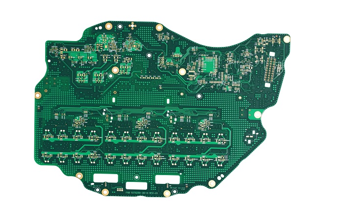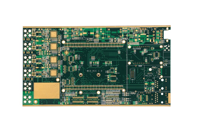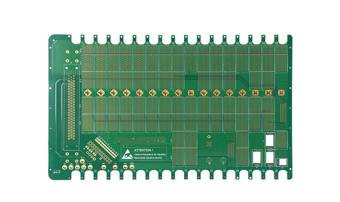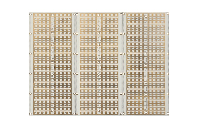
Rigid Multilayer
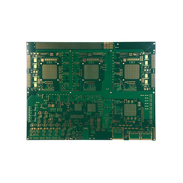
2–30 layers with impedance control, backdrilling and heavy copper for power and backplane designs.
Three owned plants, 130,000 m² of monthly capacity and 1,500 people behind every order — from a five-piece prototype to a 16-layer backplane running in volume. Quoted in 4 hours, engineered before it is priced.
IATF 16949 · ISO 13485 · ISO 9001 · ISO 14001 · UL
Bare board, assembly and components under one roof means one point of accountability when something goes wrong — not three suppliers pointing at each other.
2–30 layers with impedance control, backdrilling and heavy copper for power and backplane designs.
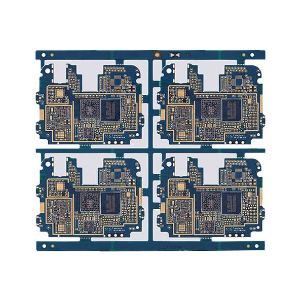
1+N+1 through any-layer build-ups, up to six sequential laminations, 0.075 mm laser vias.
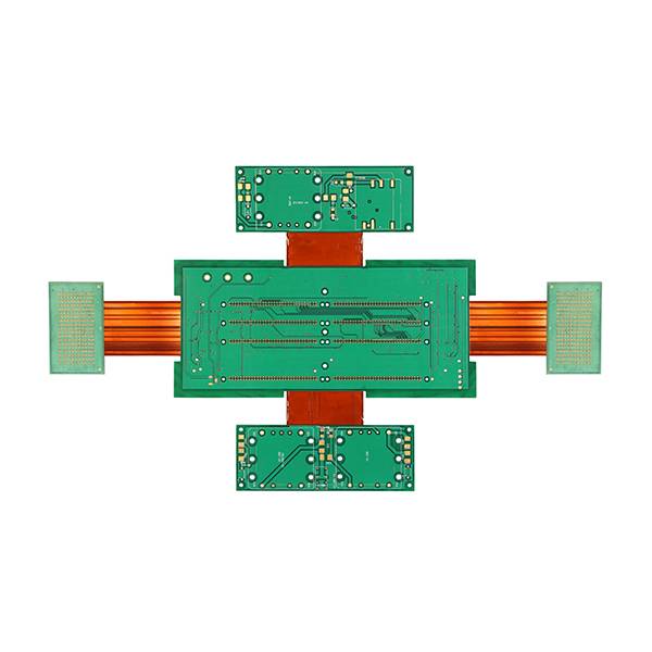
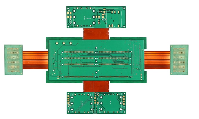
FPC from 1 to 8 layers, rigid-flex to 16 layers, including rigid-flex with metal backing.
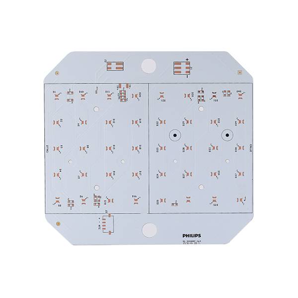
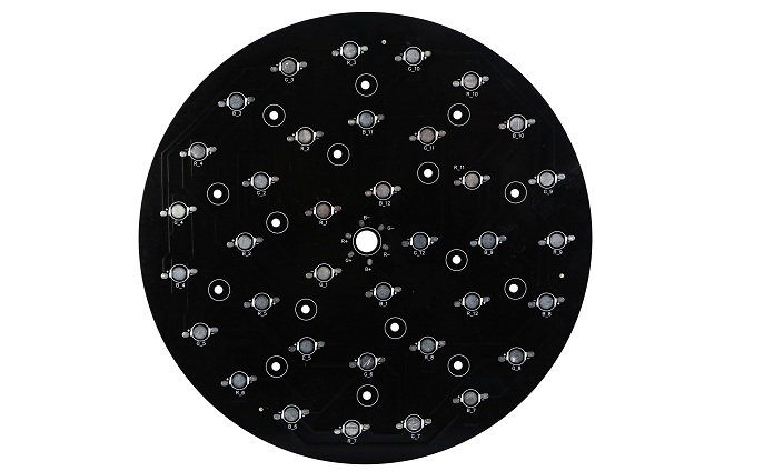
Aluminium and copper substrates for LED, power conversion and thermal-critical assemblies.
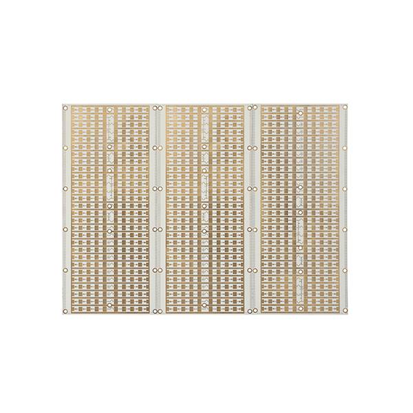
Rogers, Taconic and Arlon laminates, including FR4 hybrid stack-ups for RF and antenna boards.
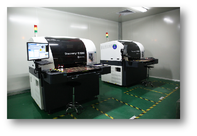
Six SMT lines, 6 million solder joints a day, 03015 chip and 0.35 mm pitch BGA capability.
Standard means we run it every week. Best-in-class means we have shipped it and will quote it after an engineering review — not that we hope it works.
Special stack-ups — buried capacitance, embedded coin, rigid-flex with metal base, backdrilling and stepped slots — are quoted after engineering review. Full material list: TUC, ITEQ, Nanya, SYL, Isola, Rogers, Arlon, Nelco, Taiflex, DuPont.
Every order is traced through the same routing, with 100% final inspection before shipment.
Panelised to the stack-up, lot-tagged on arrival.
Dry film, exposure, DES and AOI on every panel.
Brown oxide, lay-up and vacuum hot press to the build.
CNC and laser drilling, hole accuracy ±0.075 mm.
PTH, panel plating and pattern plating with thickness control.
LDI exposure and etching to 3/3 mil.
Screen print, exposure, development, IR cure.
ENIG, HASL, OSP, immersion silver or tin.
Flying probe and dedicated fixture test.
AVI, 100% FQA and microsection on request.
CNC routing, V-cut and chamfer to tolerance.
Vacuum, desiccant, lot documentation, ship.
Quick-turn work stays in Shenzhen where the engineers and SMT lines are. Volume moves to Zhongshan. Cost-sensitive programmes run in Jiangxi.
| Layers | Sample < 1 m² | 1–5 m² | 5–10 m² |
|---|---|---|---|
| 2 layers | 5 | 7 | 10 |
| 4 layers | 5 | 7 | 10 |
| 6 layers | 8 | 10 | 14 |
| 8 layers | 8 | 12 | 14 |
| 10 layers | 10 | 10 | 14 |
| 12 layers | 12 | 14 | 17 |
| 16 layers | 15 | 17 | 20 |
| 20 layers | 20 | 22 | 25 |
Automotive control units, medical devices, photovoltaic backplanes, defence electronics. The common requirement is not price — it is that nothing fails after installation.
Certificate numbers and issuing bodies are supplied with every RFQ pack. Buyers are welcome to verify them, and to schedule a video or on-site audit.
AOI after inner-layer imaging, AVI after surface finish, flying-probe electrical test on every panel, ionic contamination and microsection in the in-house lab, then 100% FQA before packing. Reports ship with the boards, not on request.
Gerber, layer count, quantity, material and finish is enough to start. We review the stack-up for manufacturability before quoting, and tell you when a cheaper route exists.