
Three plants, each doing what it does best
Quick-turn stays in Shenzhen where the engineers and SMT lines are. Volume moves to Zhongshan. Cost-sensitive programmes run in Jiangxi.
At a glance
- Zoran operates three manufacturing sites in China with a combined capacity of 130,000 m² per month.
- Shenzhen (20,000 m²/month) handles quick-turn, high-mix low-volume and all SMT assembly.
- Zhongshan (70,000 m²/month) handles volume rigid PCB, HDI and FPC, and was established in 2011.
- Jiangxi (40,000 m²/month) handles rigid PCB and MCPCB for cost-sensitive volume, established 2014 and expanded 2017.
- Total investment across the three sites is approximately USD 95 million, with 1,500 employees.
Shenzhen
- High-mix, low-volume
- 6 SMT lines · 6M joints/day
- Established 2004
Zhongshan
- Rigid PCB · HDI · FPC
- Large-volume programmes
- Established 2011, upgraded 2013
Jiangxi
- Rigid PCB · MCPCB
- Absorbs volume peaks
- Established 2014, expanded 2017
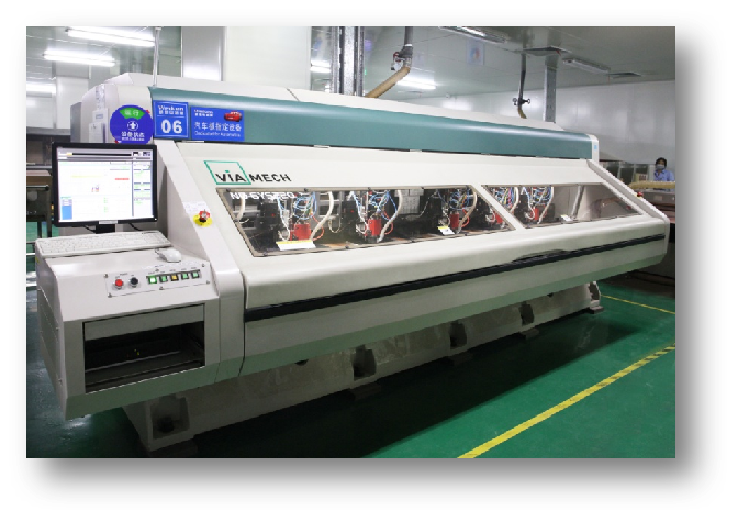
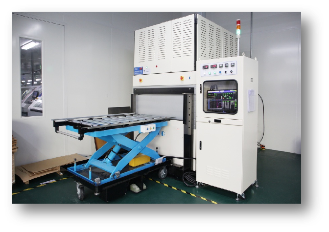
What is actually on the floor
Selected process stations. A full equipment list with models is available during a factory audit.
Total investment
Approx. USD 95 million across three sites
Founded
2004, Shenzhen — first plant and current headquarters
Employees
1,500 across manufacturing, engineering and quality
Export
46% of 2025 revenue, served through the Hong Kong office
Process flow, start to finish
Every order follows the same twelve-stage routing regardless of quantity. Panels are lot-tagged at cutting and the tag follows the board through plating, imaging and test.
- Material cutting and lot identification
- Inner-layer imaging and AOI
- Brown oxide and vacuum lamination
- CNC and laser drilling
- PTH, panel plating and pattern plating
- Outer-layer imaging and etching
- Solder mask print, expose, cure
- Surface finish — ENIG, HASL, OSP
- Electrical test and AVI
- Final quality assurance
- Profiling and V-cut
- Vacuum packing and documentation
Why three sites instead of one
A single plant cannot be simultaneously the fastest for prototypes and the cheapest for volume — the scheduling logic is different. Separating them means a quick-turn order is not queued behind a 20,000 m² programme.
In practice: prototypes and NPI in Shenzhen with the process engineers, volume transferred to Zhongshan once the part is stable, and cost-driven lighting programmes in Jiangxi from the start.
Want to see the floor before you commit?
Video walkthrough within a week, or an on-site audit in Shenzhen or Zhongshan.